Architectual.Gravitas
Advanced Engineering - military robot could feed on human bodies

eatr_robot_landscape
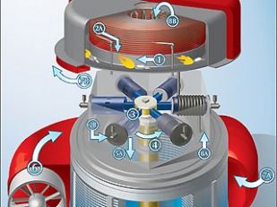
cyclone_engine
http://www.foxnews.com/story/0,2933,532492,00.html
Cyclone Power Technologies' Waste Heat Engine, which would power EATR.
- A Maryland company under contract to the Pentagon is working on a steam-powered robot that would fuel itself by gobbling up whatever organic material it can find — grass, wood, old furniture, even dead bodies.Robotic Technology Inc.'s Energetically Autonomous Tactical Robot — that's right, "EATR" — "can find, ingest, and extract energy from biomass in the environment (and other organically-based energy sources)

eatr_illo
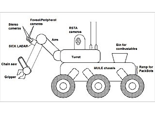
eatr_robot_diagram
=================================================================
Nanosolar is leading the “Third Wave” of solar power technology:
- Nanosolar -- brings together the entire conjunction of all seven areas of innovation, each break-through in their own right, to deliver a dramatic improvement in the cost-efficiency, yield, and throughput of the production of much thinner solar cells.

Nanosolar is a global leader in solar power innovation. We are setting the standard for affordable green power with solar cell technology of distinctly superior cost efficiency, versatility, and availability.
Our mission is very simple: Delivering cost-efficient solar electricity.
Leveraging recent science in nanostructured materials, we have developed a critical mass of engineering advances that profoundly change the cost efficiency and production scalability of solar electricity cells and panels.
Our first product, the Nanosolar Utility Panel™ enables unprecedented system economics at utility scale.
Founded in 2002, we are building the world's largest solar cell factory in California and the world's largest panel-assembly factory in Germany.
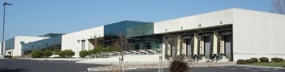
Nanosolar 200,000 SQFT FACILITY SanJose,CALI

Nanosolar's 500,000 sqft manufacturing site nearr Berlin
http://www.nanosolar.com/technology.htm

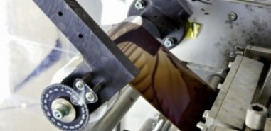
nanoparticle ink
Leveraging recent science advances in nanostructured materials, Nanosolar has developed a proprietary ink that makes it possible to simply print the semiconductor of a high-performance solar cell. This ink is based on Nanosolar developing various proprietary forms of nanoparticles and associated organic dispersion chemistry and processing techniques suitable for delivering a semiconductor of high electronic quality.
A key advantage of the ink is specific to an idiosyncracy of the CIGS semiconductor: Because it consists of four elements which have to be in just the right atomic ratios to each other, the ink serves a useful purpose by effectively "locking in" a uniform distribution ("by design"). The homogeneous mix of nanoparticles in the ink in just the right overall amounts ensures that the atomic ratios of the four elements are correct wherever the ink is printed, even across large areas of deposition. This contrasts to vacuum deposition processes where, due to the four-element nature of CIGS, one effectively has to "atomically" synchronize various materials sources -- a challenge with no successful precedent in any industry on a repeatable high-yield production-scale basis.
SEMICONDUCTOR PRINTING
printsemi
Printing is by far the simplest, highest-yield, and most capital-efficient technique for depositing thin films. Printing is extremely fast; the equipment involved is easy to use and maintain; and it works in plain air (no vacuum chamber required).Another key advantage of a printable CIGS ink is that one can print it just where one wants it to be, achieving high materials utilization of the semiconductor material. Printing is much simpler and more robust than vacuum deposition techniques such as sputtering or evaporation which have conventionally been used to fabricate thin-film solar cells; the process cost of vacuum techniques is so high that the result is not an inexpensive cell relative to the per-square-meter economics that the solar industry requires.
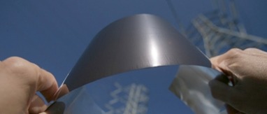
CONDUCTIVE SUBSTRATE

widefoil
Nanosolar is the first and so far only company in the world that has managed to make efficient solar cells work on a metal foil substrate that is both low cost and highly conductive. Our metal foil has a conductivity that is more than 20 times higher than that of the stainless steel used by others -- and thus enables major cost reduction on the solar cell's thin-film bottom electrode.
Note that a thin-film solar cell consists most fundamentally of an absorber layer (the semiconductor) sandwiched in between a top and a bottom electrode layer. If the thin films of a solar cell are deposited directly onto a highly conductive metal foil (as opposed to glass or stainless steel), then the bottom electrode gets much simpler because the substrate can do the job of carrying the current.
Note that a thin-film solar cell consists most fundamentally of an absorber layer (the semiconductor) sandwiched in between a top and a bottom electrode layer. If the thin films of a solar cell are deposited directly onto a highly conductive metal foil (as opposed to glass or stainless steel), then the bottom electrode gets much simpler because the substrate can do the job of carrying the current.
ROLL-TO-ROLL PROCESSING
Roll-to-roll processing is the manufacturing implementation framework of choice for any product with very low cost required per large areas of deposition. Rolls that are meters wide and miles long can be processed efficiently with very high throughput (and thus minimal capital cost) in equipment with a very small footprint.
A key advantage of roll-to-roll processing is that after the first few meters of initializing a new roll, the whole process hits a steady state which can then be maintained for the entire rest of the roll, resulting in very uniform deposition process parameters applied to essentially the entire (foil) substrate. This is much better than processing wafers or glass plates, which have to be moved in and out of each process station individually, introducing undesirable start-up and move-out process state variability (and cycle time cost).
Edge effects are also greatly minimized in roll processing (whereas processing glass plates or wafers requires much work and capital dealing with uniformity issues at the edges of the substrate).
LOW-COST TOP ELECTRODE
Nanosolar has developed a fundamental innovation on its solar cells' top electrode (not shown below) which has two major benefits: It supports an entire order of magnitude higher current than any past or present thin-film solar product known; and it is very low cost. Note that obtaining a good top electrode is challenging because it has to be both transparent and conductive.
SORTED-CELL ASSEMBLY
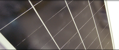
Nanosolar's approach combines the advantages of thin films with the power of electrically matched cells, resulting in better panel efficiency distribution and yield. Note that with conventional thin-film-on-glass solar technology, cell sorting and matching is not possible because cell transitions are created through scribing after they are already deposited on the glass substrate. But since each cell has somewhat different electrical characteristics, a thin-film-on-glass panel consists of cells that may not be well-matched. It turns out that the effect of electrical mismatch per cell leads to exponentially greater losses per panel as a result, and panel yield and efficiency distribution suffer: A bad cell results in a bad panel with thin-film-on-glass technology; but with a cell-sorting technology, only that cell will be a loss. The value impact of that difference is staggering: If a panel contains 100 cells, sorted-cell assembly lowers the yield-loss cost of a bad cell to 1/100th compared to monolithic cell integration.
HIGH CURRENT PANEL
With conventional silicon solar technology, individual wafer cells are sorted into performance bins before the cells are assembled into panels. This ensures that each panel produced contains cells with matched electrical characteristics.
Based on our cell and product design innovations, Nanosolar is capable of delivering high-power solar panels with 5-10 times higher current than other thin-film solar panels on the market today.
This has enabled us to work with our partners and customers to dramatically reduce the balance-of-system cost involved in deploying solar electricity systems.
The amount of current that a panel can support is important because current capacity limitations negatively impact balance-of-system cost and thus power economics.
DESIGNED TO LAST
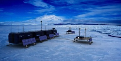
Product reliability has always been our top design priority. Our panels are rigorously tested to achieve a durability compatible with our 25-year warranty.
In fact, we test our products under much harsher conditions than mandated by official certification standards. We also expose them to harsh outdoor environments such as the Arizona desert and the Antarctic:
Accelerated lifetime testing is possible through specialized equipment that performs many -40°C to +85°C heat cycles per day, that exposes solar cells to intense UV light, and that exposes them to intense humidity. This has made it possible for us to study potential degradation mechanisms at accelerated time scale during product development.
During production, we continuously perform tests on randomly sampled production output in the form of accelerated lifetime tests under simulated high-stress conditions in indoor environmental chambers.
INVESTORS
Nanosolar is a privately held company with financial backing from an elite group of private technology investors, including:
- Premier venture funds
- Benchmark Capital -- the venture firm behind such franchise companies as eBay, Handspring, Juniper Networks and Red Hat Software;
- MDV - Mohr Davidow Ventures -- the venture firm behind such leading companies as Rambus, Epigram, FormFactor, and Agile Software;
- Leading corporations
- EDF -- the world's largest electric utility;
- AES Corporation -- one of the world's largest power producers;
- Energy Capital Partners -- a multi-billion developer of energy projects;
- Riverstone Holdings -- a multi-billion developer of energy projects of the Carlyle Group;
- Swiss Re -- the world's leading and most diversified reinsurer;
- Mitsui & Co., Ltd. -- Japan's oldest and largest international trading company with over 300 years of business presence in the world and more than $100 billion in annual business;
- Blue-chip family offices
- First Ventury -- SAP founder Klaus Tschira's investment vehicle;
- the Skoll Foundation -- formed by eBay founding President Jeff Skoll;
- the private fund by eBay founder Pierre Omidyar;
- Top-ranked hedge funds
- Lone Pine Capital -- one of the world's top ranked hedge funds;
- SAC Capital -- one of the world's leading hedge funds;
- GLG Partners -- Europe's largest hedge fund;
- LGT Capital Group -- Europe's largest wealth and asset management group;
- Grazia Equity -- the original backer of Conergy AG, the world's largest PV system integrator;
- Stanford University -- the place where many of our team members received their education;
- Individual investors including Martin Roscheisen, Sergey Brin, Carl & Larry Page, Mark Pincus, Reid Hoffman, Sunil Paul, Bernhard Beck, and Christian Reitberger.
firstpanelsshipped
PRE$$ RELEA$E$
6/2008: 1GW CIGS deposition throughput achieved.
3/2008: World's largest utility partners strategically and invests in Nanosolar.
12/2007: Nanosolar Utility Panel™ named Innovation of the Year.
12/2007: Nanosolar ships first commercial panels.
9/2007: Nanosolar awarded $20 million contract by the U.S. Department of Energy.
3/2007: Nanosolar appoints Chief Financial Officer.
1/2007: Nanosolar secures 647,000 square foot in manufacturing space.
8/2006: Conergy AG and Nanosolar sign cooperation agreement (Conergy AG press release).
6/2006: Nanosolar secures $100 million in funding ("largest greentech financing").
6/2005: Nanosolar closes Series B financing, bringing total amount of funding secured to $48 million.
8/2004: Nanosolar receives a prestigious DARPA contract in the amount of $10.3 million; U.S. Senator Boxer congratulates Nanosolar for developing "new technology to address our energy needs".
6/2003: Nanosolar confirms NY Times press report of its company formation and seed financing.
factoryconstruct
On TV / Videos:
NOVA:The Big Energy Gamble
Nanosolar:1GW Coater
CNBC:Sunshine in a Can
CNN:Global Challenges
History Channel:Modern Marvels
KQED:Solar City--The Future of Nanosolar
Nanosolar:1GW Coater
CNBC:Sunshine in a Can
CNN:Global Challenges
History Channel:Modern Marvels
KQED:Solar City--The Future of Nanosolar
White Papers / Op-Ed:
Greentech:Feeding in Renewable Energy Breakthroughs
Greenpeace Business:Silicon Valley leads solar expansion
Photon Magazine:Peer-reviewed PVSEC publication
Photon Magazine:Nanotechnology to the rescue of capital efficiency
Greenpeace Business:Silicon Valley leads solar expansion
Photon Magazine:Peer-reviewed PVSEC publication
Photon Magazine:Nanotechnology to the rescue of capital efficiency
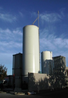
Yesterday we got our nitrogen tank installed in San Jose. It’s a big one…as is everything in this factory. nstank
"...the secret ingredient behind a new kind of technology startup that's turning heads in Silicon Valley..." [CNN article]
U.S. Senator Boxer on DARPA funding Nanosolar with $10.3 million:"This grant is exciting because it promises new technology to address our energy needs and because it again demonstrates the strength of the Bay Area's innovative private sector partnered with its world-class universities and research facilities."
The following is a partial list of recent awards and reviews:
11/2008: Nanosolar receives the prestigious "Energy Innovators" award by the U.S. Department of Energy.
10/2008: Time Magazine acknowledges Nanosolar technology as one of the Best Inventions in 2008.
9/2008: U.S. Senator Barbara Boxer presents the U.S. Senate Conservation Champion award to Nanosolar.
11/2007: Popular Science Magazine recognizes Nanosolar as the #1 innovation of 2007. Runner-up awards include the Apple iPhone and the Audi R8. See also press release.
9/2007: The U.S. Department of Energy awards the largest contract of Solar America funding ($20 million) to Nanosolar.
6/2007: The U.S. Department of Energy awards Nanosolar a $750,000 SBIR grant.
2/2007: Nanosolar named #1 company of top 20 companies pushing the ecological envelope.
11/2006: The World Economic Forum in Davos, Switzerland, names Nanosolar a Technology Pioneer.
10/2006: Inc. Magazine names Nanosolar one of the Green 50 [List].
10/2005: SmallTimes names Nanosolar one of the Top 5 Small Tech Companies [List].
7/2005: Red Herring names Nanosolar one of the Top 10 Clean Energy Companies [List].
4/2005: Nanosolar named one of the Top 100 Private Companies [List].
2/2005: Nanosolar receives $750,000 in SBIR Phase-II funding.
8/2004: Nanosolar wins the largest award in a prestigious, industry-wide DARPA competition with the goal of developing fundamentally superior solar cells. U.S. Senator Boxer congratulates Nanosolar for developing "new technology to address our energy needs".
1/2004: Nanosolar awarded Nanoelectronics grant from the National Nanotechnology Initiative.
2/2003: Nanosolar awarded a grant for innovative R&D from the California Energy Commission.
We Are Hiring!
May 4, 2009
By Martin Roscheisen CEO List of our current openings
NEW: Internships for engineering graduate students.
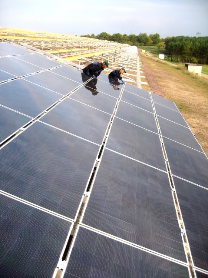
Start of Another Installation
February 12, 2009
By Martin Roscheisen CEO
May 4, 2009
By Martin Roscheisen CEO List of our current openings
NEW: Internships for engineering graduate students.
Start of Another Installation
February 12, 2009
By Martin Roscheisen CEO
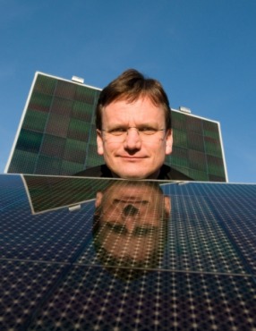
NanosolarPanelsRMRhead
United States
Headquarters & Factory
Nanosolar, Inc.
5521 Hellyer Avenue
San Jose, CA 95138
Fax: 408.365.5965
Email: [email protected] Google Map and Directions
Headquarters & Factory
Nanosolar, Inc.
5521 Hellyer Avenue
San Jose, CA 95138
Fax: 408.365.5965
Email: [email protected] Google Map and Directions
European Panel Factory
Nanosolar GmbH
Frankenfelder Chaussee 2
14943 Luckenwalde
Germany
Fax: +49.3371.68986 x100
Email: [email protected] Google Map and Directions
Nanosolar GmbH
Frankenfelder Chaussee 2
14943 Luckenwalde
Germany
Fax: +49.3371.68986 x100
Email: [email protected] Google Map and Directions
Global Press Contact
[email protected]
[email protected]
Careers
Opportunities at Nanosolar
ARTICLES
Product Design & Development, January 26, 2009
The Growing Market for Solar Cells
"Printing playing key roll in development of low-cost solar cells"
Silicon Alley Insider, January 24, 2009
VC Investing Drops for 2008, But Green Grows
"Nanosolar took the top spot in 2008"
Time Magazine, October 30, 2008
Best 50 Inventions 2008: Nanosolar
"Nanosolar named a top 50 invention"
Washington Post, September 30, 2008
Startups Best Positioned to Weather A Downturn
"Nanosolar named top company to weather economy"
USA Today, September 8, 2008
Energy Innovators: 4 creative solutions to energy problems
"Alternative energy breaking into the mainstream"
San Jose Mercury News, August 27, 2008
Thin-film solar firm Nanosolar says it has raised $300 million
"Largest amount of money raised by a solar start-up"
Venture Beat, August 27, 2008
Nanosolar outshines the competition with a $300M financing
"Nanosolar outshining competition"
Christian Science Monitor, July 9, 2008
In Silicon Valley, an economic rebound
"Nanosolar exemplifies how Silicon Valley bounced back"
Greentech Media, June 18, 2008
Nanosolar Creates Largest Thin-Film Tool
"If they've got that, they've got the world by the tail..."
Greentech Media, Apr 3, 2008
EDF Energies Nouvelles Enters Strategic Partnership with California-Based Nanosolar
EDF announces strategic partnership with Nanosolar, invests $50m
The Economist, Apr 8, 2008
Green.view: More light than heat
The New York Times, Feb 1, 2008
A Green Energy Industry Takes Root in California
"...[Nanosolar] could absolutely transform the market..."
The Salt Lake Tribune, Apr 3, 2008
Revolutionary solar technology is set to transform energy generation
Ed Firmage on the "hightechification" of energy generation
EDN, Jan 21, 2008
A Solar Panel On Every Building
"...Nanosolar's products boast an impressive list of the world's firsts"
The Guardian, Dec 29, 2007
Solar energy 'revolution' brings green power closer
"The holy grail of renewable energy..."
CNET, Dec 29, 2007
Nanosolar 'prints' first solar cells
By Michael Kanellos
San Jose Mercury News, Dec 29, 2007
Nanosolar's growing aims
By Matt Nauman
Popular Science, Nov 12, 2007
Nanosolar: Top Innovation of the Year 2007
Nanosolar named #1 innovation of the year
SF Chronicle, Sept 30, 2007
History of Silicon Valley
Sunday edition cover story by Tom Abate
CNBC, Oct 26, 2007
Big Opportunity In Nanosolar
See also video, readers' response
Earth2Tech, July 30, 2007
10 Questions for Nanosolar CEO
Earth2Tech Q&A
Forbes, July 9, 2007
Solar Power Heats Up With Nanotechnology
Forbes / Wolfe Nanotech Report
The Wall Street Journal, May 23, 2007
San Jose aiming to be 'Cleantech' capital
The city of San Jose collaborates with Nanosolar
Fortune Magazine, April 10, 2007
The Jolly Green Bubble
"Silicon Valley's premier VCs get eco-religious"
Plenty Magazine, March 17, 2007
Nanosolar: #1 of Green Energy Top 20 [Web]
"...give Nanosolar a huge jump on its competitors"
Energy and Capital, March 16, 2007
A New Day Dawns for Solar
U.S. DoE selects Nanosolar for $20m grant
Reuters, Feb 28, 2007
VentureOne: Cleantech funding doubles
Nanosolar listed as largest greentech financing in 2006
SF Chronicle, Dec 12, 2006
San Jose will have innovative solar plant
Includes photo of Nanosolar roll coater
The Motley Fool, Dec 18, 2006
A Rising Sun?
"...might even allow Nanosolar to become the dominant player in the industry"
The Economist, Nov 18, 2006
Green dreams
Editorial leader to the Nov 18th print edition
Globe and Mail, November 12, 2006
Nanosolar set for expected clean-tech boom
Shawn McCarthy in Canada's national newspaper.
Energy and Capital, Sept 19, 2006
Thin Film-Solar's Holy Grail
"...owns the best-in-class thin-film technology."
Red Herring, Aug 26, 2006
Thin Film Solar To Go Large
Article about the Conergy/Nanosolar cooperation.
CNET, June 21, 2006
With hefty funding, solar start-up takes on big guns
MIT Review, June 21, 2006
Large-Scale, Cheap Solar Electricity
"...will be able to produce solar cells much less expensively "
Renewable Energy Access, June 22, 2006
World's Largest Solar Plant Planned in Bay Area
"...will be able to produce solar cells much less expensively "
SiliconBeat, June 20, 2006
Nanosolar to build world's largest solar cell factory ...
"...has succeeded in taking far-out nanotechnology "
Red Herring, June 21, 2006
Nanosolar Gets $100M for PV
By Jennifer Kho.
San Jose Mercury News, June 21, 2006
Largest Solar Cell Factory Coming to Bay Area
By Paul Rogers.
GlobeSt, June 21, 2006
World's largest solar plant planned in Bay Area
Nanosolar choosing Bay Area location for cell factory.
Business Week, June 20, 2006
Green Growth Areas for Entrepreneurs
By Jeffrey Gangemi.
Motley Fool, Jan 20, 2006
Is the Price of Power Getting You Down?
"Unfortunately, ordinary folks can't invest in it yet."
National Geographic, Aug 2005
Powering the Future
A cover story about where the world will get its energy from.
New York Times, June 22, 2005
Green Tinge Is Attracting Seed Money to Ventures
The NY Times on investments in new solar electricity companies.
CNET, June 12, 2005
Google Founders Invest in Solar Energy
CNET Editor Michael Kanellos digs up previously unannounced information on Nanosolar's investors.
Red Herring, May 11, 2005
The Top 100 Private Companies: Nanosolar
Nanosolar named one of the Top 100 Private Companies in North America.
History Channel, Dec 30, 2004
Modern Marvels: Energy Technology [video]
Episode on "staving off the looming global energy crisis".
Fast Company, Nov 30, 2004
Green Power
"The time may finally have come for these champions of on-the-verge technologies."
San Jose Mercury News, Aug 15th 2004
World events spark interest in solar cell energy start-ups
Leader for SJMN's quarterly venture capital survey.
EE Times, Aug 15, 2004
DARPA selects contractors to develop next-generation solar cells
Nanosolar wins largest grant in competitive field of 200 companies.
USA Today / CNN / NY Times, April 26, 2004
Clean-tech firms attract growing share of venture dollars.
Associated Press about Nanosolar leading a new wave of green technology investments.
Also in CNN, NY Times.
National Public Radio, July 9, 2004
Living on Earth. Interviews with Shell Solar, Powerlight, and Nanosolar.
MIT Technology Review, June 2004
Solar-Cell Roll-Out
"Breakthroughs in nanotech are now making it possible to churn out cheap, flexible solar cells by the meter."
Forbes, Nov 24, 2003
Bright Ideas
Forbes editorial on new technologies to harness solar energy.
Newsweek, Nov 17, 2003
VCs investing in solar-cell technologies
Newsweek describes Nanosolar to report that greentech companies are now being funded by venture capitalists.
The Wall Street Journal, Aug 28, 2003
Bets are On Again
The WSJ points to Nanosolar as a first in a new market category of venture investments.
The New York Times, June 19, 2003
$6.5 Million Being Invested in a Venture on Solar Cells
http://www.nanosolar.com/blog3/
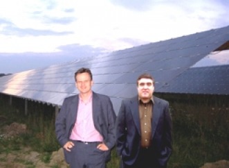
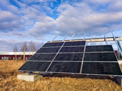
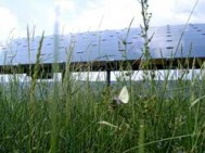
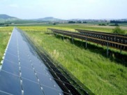
Type: Municipal Solar Power Plant. Location: Europe.
International Headquarters
Nanosolar International GmbH
Chamerstrasse 176
6300 ZUG Switzerland
Tel: +41.41.749.9942
Email: [email protected] Google Map and Directions
Nanosolar International GmbH
Chamerstrasse 176
6300 ZUG Switzerland
Tel: +41.41.749.9942
Email: [email protected] Google Map and Directions
============================================================================================
